Computational Model for Bolometer Design
Bolometers are used in a number of applications including night vision cameras, astronomy, and particle physics to measure the power of incident electromagnetic radiation. The principle of operation is shown in Figure 1: when a strip of conducting material is exposed to incident electromagnetic radiation, energy is absorbed and the temperature of the material rises. The resulting reduction in electron mobility manifests itself as a reduced electrical conductivity. If a bias current is already flowing through the strip then a reference potential is known and any change in conductivity causes a change in the reference potential which can be related to the amount of incident electromagnetic radiation. Depending on the rate of change in the material’s electrical resistance with temperature and specifics of the bolometer design, temperature changes less than 0.0001°C can be detected. To explore the effect of bolometer designs on detection of incident electromagnetic radiation, a parameterized computational model of a bolometer was developed using COMSOL Multiphysics ®. The geometry and material definitions are shown in Figure 1
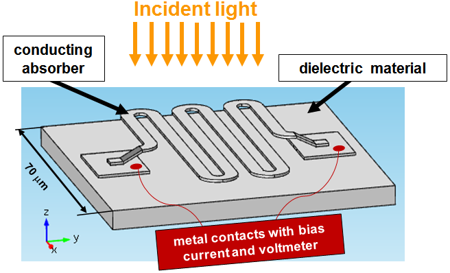
The functioning of these devices is based on three main physical phenomena: radiation through the ambient environment, heat transfer within the solid parts and conservation of electric currents. Because of the multiphysics nature of the device, COMSOL Multiphysics is well-suited for modeling, testing, and designing these devices. When the incident electromagnetic radiation is associated with sunlight the external radiation source can be defined via the solar position option in which the direction and intensity of the sun’s incident radiation is based on the latitude and longitude position on the Earth, the date, and the time. For modeling the actual bolometer, the heat transfer and electric currents equations are coupled together and solved simultaneously because of their intimately coupled nature. The bi-directional couplings are:
- The electrical conductivity: σ, is temperature dependent
- The resistive heating, Q, is a function of the voltage gradient; this is also known as Joule heating
Figure 2 shows schematically how the equations are linked; the heating term, Q, also includes a contribution from the incident light on the top boundary of the strip which drives the functioning of the device.

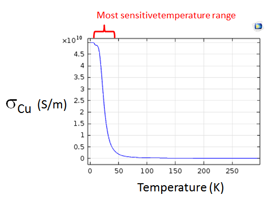
Bolometers show greatest sensitivity when operating in a regime in which the absorbing strip material shows a strong dependence of conductivity to temperature. Depending on the material chosen for the absorbing strip, some bolometers may be more sensitive when operated at cryogenic temperatures. The results shown here are for a copper material which shows a strong dependence of conductivity to temperature in the 10-50 K range (see Figure 3). This bolometer is most sensitive when the operating temperatures are kept within this range. In contrast, specialty materials that are conductivity-sensitive at room temperatures are also available.
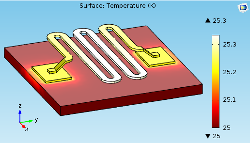
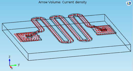
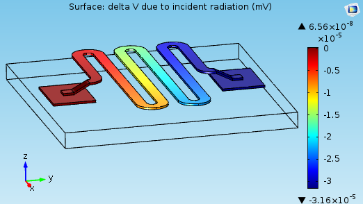
Results for analysis performed here are presented below for temperature (Figure 4), current flow (Figure 5), and the change in voltage due to the sun’s heating off the top boundary of the strip (Figure 6).
An important design parameter for bolometers is sensitivity, S, defined as change in voltage divided by amount of incident light wattage absorbed.
Good bolometer design seeks to maximize the sensitivity of these devices. Research has shown a number of design parameters can have an effect on sensitivity including the strip spacing, surface area of the strip, aspect ratio of the strip, material selection, as well as the operating temperature of the bolometer1. The loft feature available with the COMSOL Multiphysics v5.0 Design Module add-on enables the parametrization of the strip spacing parameter defined in Figure 7.
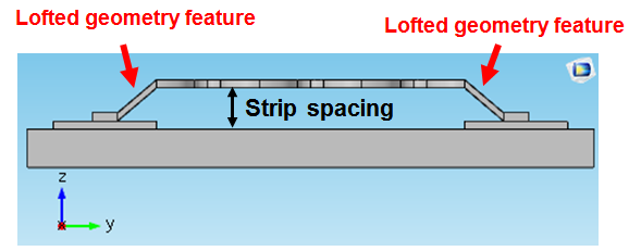
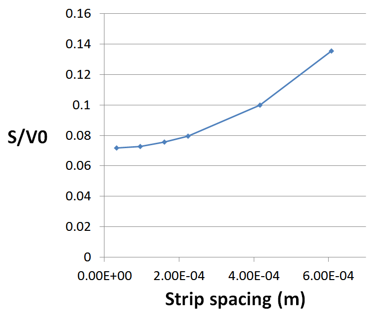
The effect of strip spacing can be seen in Figure 8, with increasing space between the mounting board and the serpentine absorber the sensitivity of the bolometer increases. This phenomenon is consistent with the operation of the device that seeks to establish the conducting absorber as a thermal isolator.
Extensions of studies of this type have been used to develop customized bolometer designs to meet the requirements of specific application.
Reference:
Stockhausen, Axel, “Optimization of Hot-Electron Bolometers for THz Radiation,” KIT Scientific Publishing, June 2013

